- Shared above-gap energy pool
- WSe2 gets only ~0.6% ideal current gain
- Thick TMDs favor ~1.0 eV gaps
- Cooling leaks can wipe out hot-carrier gains
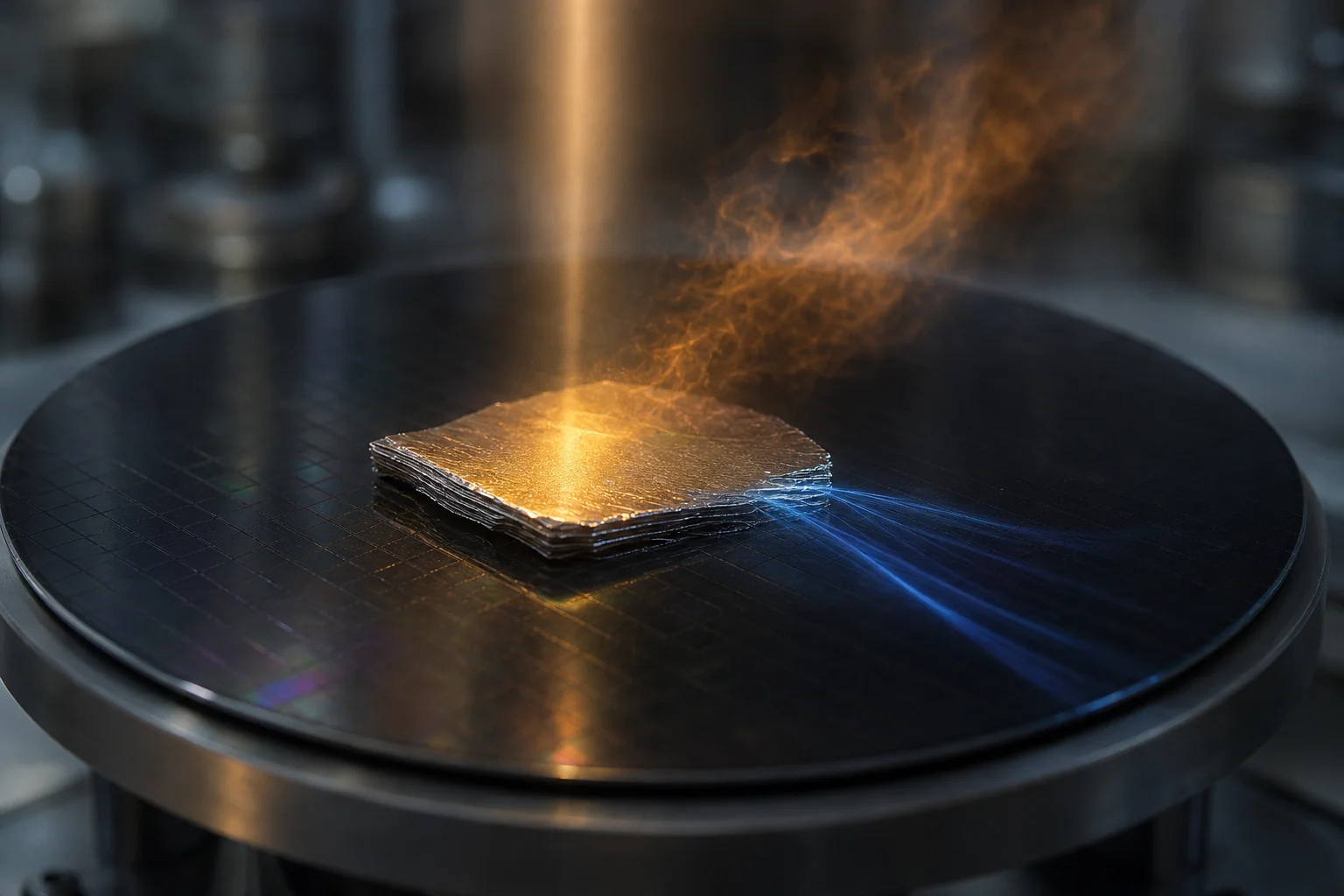
If you were hoping ultra-thin solar cells could squeeze extra power from wasted heat, this paper puts hard limits on that dream. The study looks at transition-metal dichalcogenides, a class of materials prized for strong light absorption and flexible device designs. It shows that carrier multiplication, where one energetic photon creates more than one electron, and hot-carrier extraction both pull from the same above-gap energy pool. That means carrier multiplication does not lift the reversible hot-carrier thermodynamic ceiling. The model folds in thickness-dependent absorptance, monolayer exciton effects, a carrier-multiplication quantum-yield limit of 0.97, and finite cooling leakage. For thick TMD absorbers under AM1.5G sunlight, the Shockley–Queisser optimum sits near a 1.3 eV band gap, while the carrier-multiplication and hot-carrier-friendly envelope shifts toward 1.0 eV and can exceed 50% reversible efficiency. But for monolayer WSe2 with a 1.63 eV gap, only about 3.7% of above-gap photons have enough energy for multiplication, so the ideal short-circuit-current gain is only about 0.6%. The takeaway is sharp: high-gap monolayer TMDs are poor one-sun carrier-multiplication candidates, while narrow-gap bulk-like TMDs only look promising if energy-selective extraction and suppressed cooling can be achieved together.
WSe2 has a 1.63 eV band gap. Under one-sun AM1.5G light, only about 3.7% of above-gap photons carry enough extra energy for carrier multiplication. That tiny slice matters. Carrier multiplication and hot-carrier extraction draw from the same spare energy. One does not rescue the other. If you hoped thin solar cells could squeeze more power from waste heat, this study draws a hard line. High-gap monolayers leave too little room for the trick to work. Even before real losses, the extra current gain stays tiny. For a reader, that means the shiny promise of more from the same sun has a strict size limit. Thickness and band gap set that limit from the start.
How the energy budget is counted
The model starts with detailed balance. That is a bookkeeping rule for sunlight in and heat out. It then lets light capture change with thickness. A single TMD sheet and a 10 to 50 nm stack do not swallow the same light. The model also adds excitons, the bound electron-hole pairs that shape monolayer absorption. Then it tests two upgrade paths. Carrier multiplication can split one energetic photon into several charges. Hot-carrier extraction can pull those charges out before they cool. The surprise is blunt. Both paths spend the same above-gap energy reserve. So carrier multiplication does not raise the reversible hot-carrier ceiling. AM1.5G is the standard lab sun spectrum. For thick TMDs under AM1.5G sunlight, the usual Shockley-Queisser ceiling sits near 1.3 eV. The CM and HC friendly envelope shifts toward about 1.0 eV. There, reversible efficiency rises above 50%.
Why atom-thin layers run out of room
The framework builds three pieces into one limit. First, it uses absorptance, how much light a layer swallows, and lets it depend on photon energy and thickness. Second, it treats monolayer excitons, the bound pairs that dominate atom-thin optics. Third, it caps carrier multiplication at 0.97 quantum yield. That is the number of charges per absorbed photon. For hot-carrier cells, it imagines ideal energy-selective contacts, exits that only let the right energy through. It also uses a finite heat-leak coefficient, a measure of how fast heat escapes. A resource-counting proof then shows why the two upgrade paths compete for the same excess energy.
WSe2 under AM1.5G
before device nonidealities- The model tracks thickness-dependent absorptance across photon energies.
- It includes monolayer excitons, the bound pairs that shape absorption.
- It caps carrier multiplication at a 0.97 quantum-yield limit.
- It adds ideal energy-selective contacts and a finite heat leak.
“CM and HC draw on the same above-gap photon-energy reservoir.”
Why the cooling bill stays high
For monolayer TMDs, the message is harsh. High-gap sheets are not good one-sun carrier-multiplication candidates. WSe2 is the clearest example. At 1.63 eV, it leaves almost no room above twice the band gap. Bulk-like TMDs tell a different story. At 10 to 50 nm, hot-carrier gains can become large. But the cooling bill stays huge. Even a heat-leak coefficient of 0.2 watts per square meter per kelvin still looks small. At a 500 kelvin gap, it means about 100 watts per square meter leak. That is an ambitious suppression target. So the useful path is narrow. It needs energy-selective extraction and slower heat loss at the same time.
What a serious test would need to show
The surprise leaves a clear test. A narrow-gap bulk-like TMD absorber must pair with energy-selective contacts. It also needs phonon engineering, which shapes crystal vibrations that carry heat. The hard case is a 10 to 50 nm device under one sun. It must hold down the cooling leak while keeping the hot-carrier edge. Without that pairing, carrier multiplication stays a side show. It cannot lift the hot-carrier ceiling on its own. That is the real design lesson here. Stop asking extra photon splitting to do a heat job. Give the hot electrons a path out and keep the lattice from stealing the prize.
Comments