- A 0.5 nm silicide template cuts vertical resistance
- The same trick works with 25 metals
- An amorphous-like interlayer eases lattice mismatch
- MOCVD overgrowth can build on the template
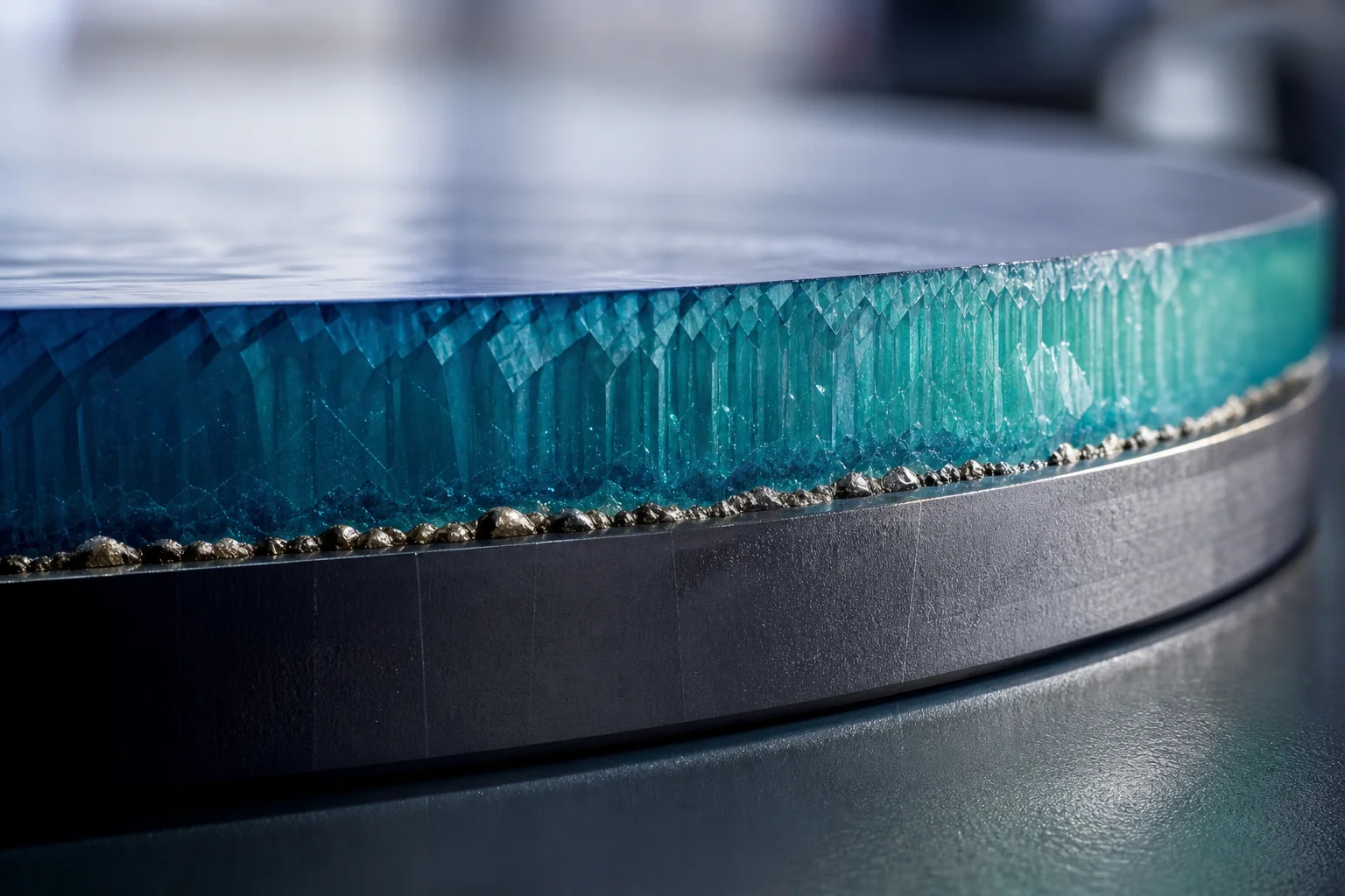
If you want gallium nitride devices on cheap silicon wafers, the usual buffer layers have been the bottleneck. They block current and make vertical designs harder to use in practice. This paper reports a sputtering-based strategy that forms an in-situ silicide-based template only about 0.5 nanometers thick, then uses rapid thermal annealing to turn it into a base for high-quality GaN growth on Si(111). The approach worked across 25 different metallic species and produced GaN films with very low vertical resistance, ohmic behavior, and strong thermal stability. Scanning transmission electron microscopy showed a unique amorphous-like interlayer that absorbs lattice mismatch and relaxes epitaxial strain. The same template also served as a strong platform for MOCVD overgrowth, which matters because it links low-cost fabrication with device-grade vertical performance for power electronics and high-resolution micro-LEDs.
A layer about 0.5 nanometers thick can decide whether current flows cleanly or stalls. That tiny gap matters for vertical GaN devices on silicon. GaN, or gallium nitride, is a hard-working semiconductor used for power tools and bright displays. Silicon is cheap and common. The catch sits between them. Thick buffer layers can block vertical current and spoil the device. This study tackles that bottleneck with a thin silicide-based template made by sputtering and rapid heat treatment. The result is a small change with a large prize. It points toward GaN chips on silicon wafers that waste less energy and are easier to scale.
The wafer-thin bridge that lets current pass
The main result is simple to state and hard to pull off. The new template supports GaN epitaxial films, which means crystal layers grown so their atoms line up with the base below. On Si(111), a common silicon face, the films show very low vertical resistance, ohmic behavior, and strong heat stability. Ohmic behavior means current rises in a smooth, straight way as voltage rises. That is what device makers want. The abstract also says the method works across 25 different metallic species. That range makes the strategy feel less like a one-off trick and more like a general tool. STEM, a sharp imaging method that looks deep inside materials, reveals why it works. The interface forms an amorphous-like interlayer that soaks up mismatch and eases strain.
How a thin metal layer becomes a crystal-friendly base
The process starts with sputtering, a way to fire atoms from a metal target onto a surface. Then rapid thermal annealing, or very fast heating and cooling, turns that film into a silicide template. A silicide is a compound made from silicon and a metal. The paper says the template forms in situ, which means it appears right on the wafer during the process. That step builds a sub-nanometer base before GaN growth begins. Later, metalorganic chemical vapor deposition, or MOCVD, grows more GaN on top. In plain terms, the template acts like a smart cushion. It keeps the layers aligned well enough for crystal growth, yet soft enough to handle the size gap between silicon and GaN.
silicide-based base layer
ultrathin interface“a unique amorphous like interlayer (AL-IL) effectively accommodates lattice mismatch and relaxes epitaxial strain.”
That one interface does more than hold two materials together. It gives the silicon side and the GaN side a way to meet without tearing each other apart. Lattice mismatch means the atoms in two crystals do not fit the same way. When that mismatch is too sharp, defects pile up and current gets worse. The amorphous-like interlayer helps by acting less like a rigid wall and more like a soft landing pad. The paper also says the templates work as strong platforms for MOCVD overgrowth. That matters because the growth method is already common in industry. A better base can therefore fit into existing paths instead of demanding a whole new factory.
Why this matters for power chips and micro-LEDs
The prize here is not only a nicer lab sample. Vertical GaN-on-silicon architectures aim at two big targets: power electronics and micro-LEDs. Power devices need low loss and high power handling. Micro-LEDs want fine pixel control and low cost. Silicon wafers already offer scale and lower cost than many other options. The trouble has been the buffer stack between GaN and silicon. If that stack blocks vertical flow, the whole idea loses force. This template attacks that weak spot directly. It also offers thermal stability, so the interface keeps its shape under heat. That is a key trait for real devices, where hot spots are normal and reliability matters.
What still has to hold up next
The next test is simple to name and hard to fake. The template must keep working as GaN films grow into full device stacks on Si(111). It also has to stay low in resistance after later device steps and heat stress. The paper already points to one useful sign. The same AL-IL template supports MOCVD overgrowth. That makes the path toward device-grade vertical performance look more practical. The open question is not whether a thin bridge can form. It is whether that bridge can stay clean, stable, and useful when the whole chip gets built on top of it.
Comments