- GHz waves travel on LAO/STO at room temperature
- Very low loss helps the signal survive
- AAFM images the wave shape in place
- The wave looks shear horizontal
- STO may link SAWs to many other materials
If you want to move single electrons with the precision quantum devices need, you need a tiny traveling conveyor belt. Surface acoustic waves, or SAWs, provide that moving electrical potential, and this paper shows they can run on LaAlO3/SrTiO3 at room temperature. The team observed SAW modes up to 2.2 GHz with very low propagation loss, about 10^-3 dB per wavelength. To see the wave forms directly, they used atomic acoustic force microscopy and achieved sub-micron resolution imaging. Their measurements point to a shear horizontal-type mode, which can couple to in-plane degrees of freedom. That matters because the LAO/STO interface hosts a gate-tunable superconducting two-dimensional electron gas that can be programmed into devices such as ballistic electron waveguides and quantum dots. The work also sheds light on how SAWs are generated in strontium titanate, a widely used and commercially available substrate, and suggests a route for coupling SAWs to materials grown or transferred onto it.
A wave that moves like a tiny conveyor belt now runs on a surface that should make that hard. The surface is LaAlO3/SrTiO3, often called LAO/STO. It hosts a gate-tuned two-dimensional electron gas, or 2DEG, which is a very thin layer of mobile charge. That layer can form quantum devices such as electron waveguides and quantum dots. The surprise is simple. Even though SrTiO3 lacks the usual room-temperature piezoelectric trick, the surface still carries gigahertz waves. The paper reports modes up to 2.2 GHz. It also reports very low loss. That matters because a clean wave can carry single electrons or paired electrons without dropping them along the way.
A wave that can carry charge without much drag
The cleanest result is the wave itself. LAO/STO supports surface acoustic wave modes up to 2.2 GHz. Surface acoustic waves, or SAWs, are ripples that travel along a solid's skin. In this case, the ripples also carry an electrical pattern that can catch electrons. The loss stays tiny, at about 10^-3 dB per wavelength. That means the wave fades very slowly as it moves. The paper points to a shear horizontal-type mode. In plain terms, the motion runs sideways rather than straight up and down. That side-to-side motion can couple to in-plane degrees of freedom, which are the motions inside the surface plane. For future quantum devices, that is a useful fit.
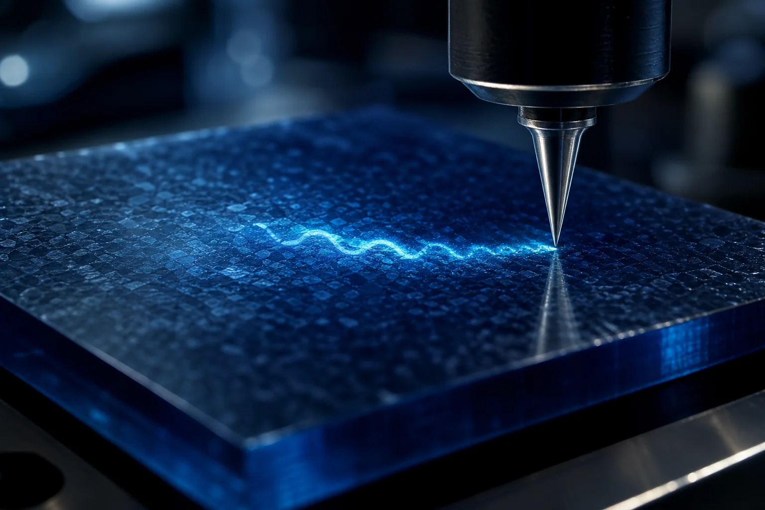
How the wave was brought into view
The key tool is atomic acoustic force microscopy, or AAFM. It is a scanning probe method that feels motion on a surface with a very sharp tip. The tip gives sub-micron resolution, so it can map wave shapes that are smaller than a human hair. That matters here because the wave is not just a number from an electrical readout. It is a shape moving across the surface. The imaging gives direct proof of the wave form, not just hints from a circuit trace. The authors use that view to link the observed motion to electrostriction. Electrostriction means a material changes shape when an electric field pulls on it. Here, that effect helps launch the SAW in STO at room temperature.
room-temperature SAW mode in LAO/STO
directly imaged by AAFM- The interface can host single electrons, electron pairs, and other exotic states.
- SAWs can shuttle those charges between spatially separated devices.
- STO can serve as a common substrate for many grown or transferred materials.
“To directly visualize these modes, we employ Atomic Acoustic Force Microscopy (AAFM), achieving sub-micron resolution imaging of the SAW wave forms.”
“very low propagation loss of the order 10−3 dB per wavelength”
Why this matters for quantum transport
The LAO/STO interface already gives device builders a tunable quantum playground. The new wave adds a transport tool. A SAW can act like a moving pocket that picks up an electron and carries it onward. That is the basic trick behind acoustoelectric transport. It becomes useful when devices sit apart from each other on the same chip. The paper's message is not that the whole quantum system is finished. It is narrower and stronger. The substrate itself can now support fast SAWs at room temperature. That makes STO a more flexible base for acoustics and quantum layouts. It also opens coupling routes to materials that can grow on STO or be moved onto it.
What to test next on STO
The next test is clear. The same SAWs need to work with real device structures on STO, not only with the bare surface response. The paper points to quantum transport uses such as ballistic electron waveguides and quantum dots. It also points to single electrons, electron pairs, and other exotic states as the target cargo. The strongest open question is whether the shear horizontal mode can couple cleanly to those in-plane states in a working device. If it does, a room-temperature SAW line on STO could become a practical bridge between separate quantum parts. That would turn a hard-to-believe surface wave into a routing tool for future chips.
Comments